03. Memory
术语
时钟(Clock)基于振荡器在低电平-高电平之间交替变化,提供连续的交变信号序列。两个相邻的上升沿之间的时间间隔称为一个周期(Cycle),周期的倒数即为频率(Frequency)。
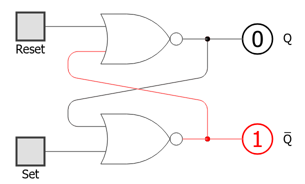
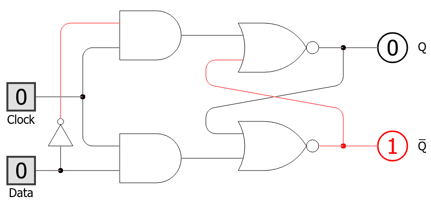
触发器(Flip-Flops)计算机中最基本的时序单元。
寄存器(Registers)具有记忆功能的设备,能够存储某一时刻的值。基本设计参数是宽度(Width)即它能够存储的比特位数,比如 16,32 或 64 位。此类寄存器的多位容量通常用字(Word)来表示。
内存(Memories)可以通过将很多寄存器堆叠起来形成随机存取内存(Random Access Memory,RAM)。每个寄存器都有一个地址(Address),可以通过地址访问特定的寄存器。基本设计参数是它的数据宽度(即每个字的宽度)和它的大小(RAM 中字的数量)。
Chip API
通过递归组合逐步构建内存块,一个 w-bit 的寄存器由 w 个 1-bit 寄存器构成,RAM8 内存块由 8 个 w-bit 寄存器构成,RAM64 内存块由 8 个 RAM8 内存块构成,以此类推。
chip
芯片名:  DFF
输入:    int
输出:    out
功能:    out(t) = in(t-1)
说明:    DFF 有现成的内置实现版本,无需自己实现。
chip
芯片名:  Bit
输入:    in, load
输出:    out
功能:    if load(t-1) then out(t) = in(t-1)
         else out(t) = out(t-1)
chip
芯片名:  Register
输入:    in[16], load
输出:    out[16]
功能:    if load(t-1) then out(t) = in(t-1)
         else out(t) = out(t-1)
chip
芯片名:  RAMn    // n 和 k 在以下有说明
输入:    in[16], load, address[k]
输出:    out[16]
功能:    out(t) = RAM[address(t)](t)

用于 Hack 平台的具体 RAM 芯片如下:

芯片名           n          k
RAM8            8          3
RAM64          64          6
RAM512        512          9
RAM4K        4096         12
RAM16K      16384         14
chip
芯片名:  PC    // 16-bit 的计数器
输入:    in[16], load, inc, reset
输出:    out[16]
功能:    if reset(t-1) then out(t) = 0
         else if load(t-1) then out(t) = in(t-1)
         else if inc(t-1) then out(t) = out(t-1) + 1
         else out(t) = out(t-1)
触发器
https://www.codehiddenlanguage.com/Chapter17
Project 03
load 是理解内存芯片的关键:它不是要不要输出,而是要不要在下一个时钟周期更新保存的值。输出一直存在,只是当 load=0 时继续保持旧值。
hdl
/**
 * 1-bit register:
 * If load is asserted, the register's value is set to in;
 * Otherwise, the register maintains its current value:
 * if (load(t)) out(t+1) = in(t), else out(t+1) = out(t)
 */
CHIP Bit {
    IN in, load;
    OUT out;

    PARTS:
        Mux(a=feedback, b=in, sel=load, out=next);
        DFF(in=next, out=feedback, out=out);
}
hdl
/**
 * 16-bit register:
 * If load is asserted, the register's value is set to in;
 * Otherwise, the register maintains its current value:
 * if (load(t)) out(t+1) = int(t), else out(t+1) = out(t)
 */
CHIP Register {
    IN in[16], load;
    OUT out[16];

    PARTS:
        Bit(in=in[0], load=load, out=out[0]);
        Bit(in=in[1], load=load, out=out[1]);
        Bit(in=in[2], load=load, out=out[2]);
        Bit(in=in[3], load=load, out=out[3]);
        Bit(in=in[4], load=load, out=out[4]);
        Bit(in=in[5], load=load, out=out[5]);
        Bit(in=in[6], load=load, out=out[6]);
        Bit(in=in[7], load=load, out=out[7]);
        Bit(in=in[8], load=load, out=out[8]);
        Bit(in=in[9], load=load, out=out[9]);
        Bit(in=in[10], load=load, out=out[10]);
        Bit(in=in[11], load=load, out=out[11]);
        Bit(in=in[12], load=load, out=out[12]);
        Bit(in=in[13], load=load, out=out[13]);
        Bit(in=in[14], load=load, out=out[14]);
        Bit(in=in[15], load=load, out=out[15]);
}
hdl
/**
 * Memory of eight 16-bit registers.
 * If load is asserted, the value of the register selected by
 * address is set to in; Otherwise, the value does not change.
 * The value of the selected register is emitted by out.
 */
CHIP RAM8 {
    IN in[16], load, address[3];
    OUT out[16];

    PARTS:
        DMux8Way(in=load, sel=address, a=load0, b=load1, c=load2, d=load3, e=load4, f=load5, g=load6, h=load7);
        Register(in=in, load=load0, out=out0);
        Register(in=in, load=load1, out=out1);
        Register(in=in, load=load2, out=out2);
        Register(in=in, load=load3, out=out3);
        Register(in=in, load=load4, out=out4);
        Register(in=in, load=load5, out=out5);
        Register(in=in, load=load6, out=out6);
        Register(in=in, load=load7, out=out7);
        Mux8Way16(a=out0, b=out1, c=out2, d=out3, e=out4, f=out5, g=out6, h=out7, sel=address, out=out);
}
hdl
/**
 * Memory of sixty four 16-bit registers.
 * If load is asserted, the value of the register selected by
 * address is set to in; Otherwise, the value does not change.
 * The value of the selected register is emitted by out.
 */
CHIP RAM64 {
    IN in[16], load, address[6];
    OUT out[16];

    PARTS:
        DMux8Way(in=load, sel=address[3..5], a=load0, b=load1, c=load2, d=load3, e=load4, f=load5, g=load6, h=load7);
        RAM8(in=in, load=load0, address=address[0..2], out=out0);
        RAM8(in=in, load=load1, address=address[0..2], out=out1);
        RAM8(in=in, load=load2, address=address[0..2], out=out2);
        RAM8(in=in, load=load3, address=address[0..2], out=out3);
        RAM8(in=in, load=load4, address=address[0..2], out=out4);
        RAM8(in=in, load=load5, address=address[0..2], out=out5);
        RAM8(in=in, load=load6, address=address[0..2], out=out6);
        RAM8(in=in, load=load7, address=address[0..2], out=out7);
        Mux8Way16(a=out0, b=out1, c=out2, d=out3, e=out4, f=out5, g=out6, h=out7, sel=address[3..5], out=out);
}
PC 比普通 Register 多了优先级:reset、load、inc、保持不变。写的时候要先想清楚这些控制信号谁覆盖谁。
hdl
/**
 * Memory of 512 16-bit registers.
 * If load is asserted, the value of the register selected by
 * address is set to in; Otherwise, the value does not change.
 * The value of the selected register is emitted by out.
 */
CHIP RAM512 {
    IN in[16], load, address[9];
    OUT out[16];

    PARTS:
        DMux8Way(in=load, sel=address[6..8], a=load0, b=load1, c=load2, d=load3, e=load4, f=load5, g=load6, h=load7);
        RAM64(in=in, load=load0, address=address[0..5], out=out0);
        RAM64(in=in, load=load1, address=address[0..5], out=out1);
        RAM64(in=in, load=load2, address=address[0..5], out=out2);
        RAM64(in=in, load=load3, address=address[0..5], out=out3);
        RAM64(in=in, load=load4, address=address[0..5], out=out4);
        RAM64(in=in, load=load5, address=address[0..5], out=out5);
        RAM64(in=in, load=load6, address=address[0..5], out=out6);
        RAM64(in=in, load=load7, address=address[0..5], out=out7);
        Mux8Way16(a=out0, b=out1, c=out2, d=out3, e=out4, f=out5, g=out6, h=out7, sel=address[6..8], out=out);
}
hdl
/**
 * Memory of 4K 16-bit registers.
 * If load is asserted, the value of the register selected by
 * address is set to in; Otherwise, the value does not change.
 * The value of the selected register is emitted by out.
 */
CHIP RAM4K {
    IN in[16], load, address[12];
    OUT out[16];

    PARTS:
        DMux8Way(in=load, sel=address[9..11], a=load0, b=load1, c=load2, d=load3, e=load4, f=load5, g=load6, h=load7);
        RAM512(in=in, load=load0, address=address[0..8], out=out0);
        RAM512(in=in, load=load1, address=address[0..8], out=out1);
        RAM512(in=in, load=load2, address=address[0..8], out=out2);
        RAM512(in=in, load=load3, address=address[0..8], out=out3);
        RAM512(in=in, load=load4, address=address[0..8], out=out4);
        RAM512(in=in, load=load5, address=address[0..8], out=out5);
        RAM512(in=in, load=load6, address=address[0..8], out=out6);
        RAM512(in=in, load=load7, address=address[0..8], out=out7);
        Mux8Way16(a=out0, b=out1, c=out2, d=out3, e=out4, f=out5, g=out6, h=out7, sel=address[9..11], out=out);
}
hdl
/**
 * Memory of 16K 16-bit registers.
 * If load is asserted, the value of the register selected by
 * address is set to in; Otherwise, the value does not change.
 * The value of the selected register is emitted by out.
 */
CHIP RAM16K {
    IN in[16], load, address[14];
    OUT out[16];

    PARTS:
        DMux4Way(in=load, sel=address[12..13], a=load0, b=load1, c=load2, d=load3);
        RAM4K(in=in, load=load0, address=address[0..11], out=out0);
        RAM4K(in=in, load=load1, address=address[0..11], out=out1);
        RAM4K(in=in, load=load2, address=address[0..11], out=out2);
        RAM4K(in=in, load=load3, address=address[0..11], out=out3);
        Mux4Way16(a=out0, b=out1, c=out2, d=out3, sel=address[12..13], out=out);
}
hdl
/**
 * A 16-bit counter.
 * if      reset(t): out(t+1) = 0
 * else if load(t):  out(t+1) = in(t)
 * else if inc(t):   out(t+1) = out(t) + 1
 * else              out(t+1) = out(t)
 */
CHIP PC {
    IN in[16],inc, load, reset;
    OUT out[16];

    PARTS:
        Inc16(in=feedback, out=out1);
        Mux16(a=feedback, b=out1, sel=inc, out=out2);
        Mux16(a=out2, b=in, sel=load, out=out3);
        Mux16(a=out3, b=false, sel=reset, out=next);
        Register(in=next, load=true, out=feedback, out=out);
}